IEEE Fellow
Dr. Steven H Voldman, LLC
e-mail: voldman@ieee.org
ESD and Latchup in Three Dimensional (3-D) Semiconductor Memory Chip Systems
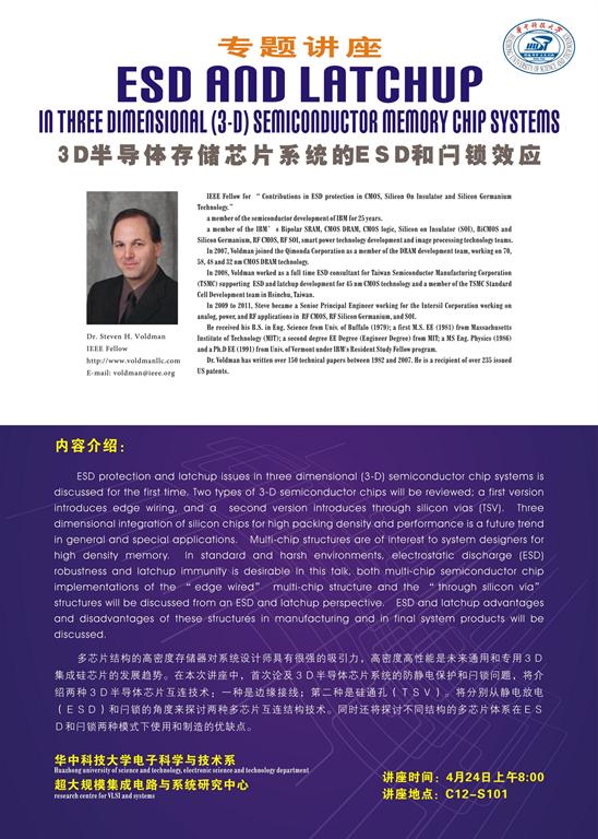
ESD protection and latchup issues in three dimensional (3-D) semiconductor chip systems is discussed for the first time. Two types of 3-D semiconductor chips will be reviewed; a first version introduces edge wiring, and a second version introduces through silicon vias (TSV). Three dimensional integration of silicon chips for high packing density and performance is a future trend in general and special applications. Multi-chip structures are of interest to system designers for high density memory. In standard and harsh environments, electrostatic discharge (ESD) robustness and latchup immunity is desirable In this talk, both multi-chip semiconductor chip implementations of the “edge wired” multi-chip structure and the “through silicon via” structures will be discussed from an ESD and latchup perspective. ESD and latchup advantages and disadvantages of these structures in manufacturing and in final system products will be discussed.
Biography
Dr. Steven H. Voldman is an IEEE Fellow for “Contributions in ESD protection in CMOS, Silicon On Insulator and Silicon Germanium Technology.” He was the recipient of the ESD Association Outstanding Contribution Award in 2007. He received his B.S. in Eng. Science from Univ. of Buffalo (1979); a first M.S. EE (1981) from Massachusetts Institute of Technology (MIT); a second degree EE Degree (Engineer Degree) from MIT; a MS Eng. Physics (1986) and a Ph.D EE (1991) from Univ. of Vermont under IBM's Resident Study Fellow program. Dr. Voldman was a member of the semiconductor development of IBM for 25 years. He was a member of the IBM’s Bipolar SRAM, CMOS DRAM, CMOS logic, Silicon on Insulator (SOI), BiCMOS and Silicon Germanium, RF CMOS, RF SOI, smart power technology development and image processing technology teams. In 2007, Voldman joined the Qimonda Corporation as a member of the DRAM development team, working on 70, 58, 48 and 32 nm CMOS DRAM technology. In 2008, Voldman worked as a full time ESD consultant for Taiwan Semiconductor Manufacturing Corporation (TSMC) supporting ESD and latchup development for 45 nm CMOS technology and a member of the TSMC Standard Cell Development team in Hsinchu, Taiwan. In 2009 to 2011, Steve became a Senior Principal Engineer working for the Intersil Corporation working on analog, power, and RF applications in RF CMOS, RF Silicon Germanium, and SOI.
Dr. Voldman was a member of the ESD Association Board of Directors, ESDA Education Committee, as well ESD Standards Chairman for TLP and VF-TLP testing. Steve has provided tutorials on ESD, and latchup to the IRPS, EOS/ESD, T-ESDC, BCTM, IPFA, ASICON (China), and ICSICT (China). In the ESD Association, Voldman initiated the “ESD on Campus” program which was established to bring ESD lectures and interaction to university faculty and students internationally; the ESD on Campus program has reached over 35 universities in the United States, Singapore, Taiwan, Malaysia, Philippines, Thailand, and many universities in China. He also provides tutorials internationally on ESD protection. Dr. Voldman is an author of six books --ESD: Physics and Devices,ESD:Circuits and Devices,ESD: Radio Frequency (RF) Technology and Circuits, Latchup, ESD: Failure Mechanisms and Models, and ESD: Design and Synthesis, as well as a contributor to the bookSilicon Germanium: Technology, Modeling and Design, and a new textNanoelectronics: Nanowires, Molecular Electronics, and Nano-devices. Dr. Voldman also has written an article forScientific Americanin October 2002. Dr. Voldman has written over 150 technical papers between 1982 and 2007. He is a recipient of over 235 issued US patents. Steven Voldman provides tutorials and lectures on inventions, innovations, and patents in Penang, Kuala Lumpur, Johor Bahru, Sri Lanka and the United States ; and has also founded a limited liability corporation (LLC) consulting business supporting ESD design, teaching, patents and patent litigation. In his LLC, S. Voldman served as an expert witness for over six cases on DRAM development, semiconductor development, integrated circuits, and electrostatic discharge.
讲座时间:4月24日上午8:30 教室:C12-S101